ETH Zurich spin-off UNISERS may play an important role in the next miniaturization step of computer chips. In any case, established semiconductor companies already working with the start-up company think so. The team is now looking for investors for the next development step.
Around 1000 production steps are needed to produce a computer chip. Up to forty percent of the chips produced are ultimately not used because of quality issues. One reason for this are tiny impurities. This problem is becoming more and more virulent as the structures on the chips become smaller and smaller. The industry is currently working on the transition to ten- or even sub-ten-nanometer structures. As a result, ever smaller impurities are sufficient to render a chip unusable. The fact that major semiconductor manufacturers have not yet reached profitable yield with the newest miniaturization steps is also due to this problem.
The solution could come out of Zurich, from the ETH spinoff UNISERS. The company has developed a particle scanner for the detection of contaminations on wafers. “Beginning of the year we were able to push the detection limit in the ten-nanometre range,” explains CTO and co-founder Fabian Walter. This gave the start-up access to the industry’s central research group. UNISERS was contacted by the International Roadmap Committee (IRDS), the group that works on the key challenges of the semiconductor industry. IRDS and UNISERS started a joint project that was so successful that one of the big-3 semiconductor manufacturers soon decided to join. It did not stop there. “We are now working on three projects with semiconductor suppliers from the USA,” says Fabian Walter.
The first affordable solution
The UNISERS product is not only convincing because of its performance. The alternatives available today either require a lot of manual work or are so expensive that hardly any manufacturer and supplier can afford them. The particle scanner from Zurich automates detection and is massively cheaper than the only competing product on the market. “For the scanner, we use components from suppliers to which we apply minor but crucial adaptations. In addition, we use software we developed ourselves,” explains the CTO.
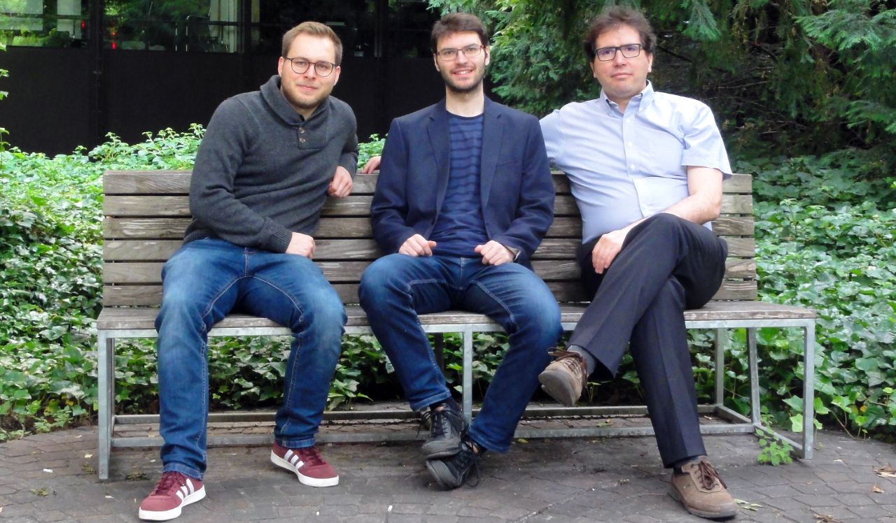
The three-member founding team covers the necessary competencies for development. CEO Ali Altun comes from nanotechnology research but has also worked for five years in the semiconductor industry. Timo Schneider, responsible for product development, is a mechanical engineer. And Fabian Walter has a software background. Support programmes such as the ETH Pioneer Fellowship Programme, Venturelab courses and Innosuisse Coaching have helped the team to acquire the necessary business skills.
This has enabled the engineers to develop an offer that is well received in the industry. “Our basic technology is very versatile,” says Fabian Walter. When the project started, the team wanted to develop a tool that would literally meet all the requirements of potential users. But development would have been too expensive and time-consuming. The team decided to simplify the tool and took to the road to success.
Strategic partnerships and bridge round
The next business goal for UNISERS is to reach the threshold of one million Swiss francs in sales. To achieve this, fresh financial resources are necessary. “We had originally planned a financing round of 1.2 million francs, but we can well imagine a Pre-Series-A financing as well,” says Fabian Walter. The new perspective has arisen because the team has been contacted by two semiconductor companies with whom they are now talking about a strategic collaboration. Pre-Series-A financing could finance the start-up until the conclusion of these partnerships. After that, in 2021, a financing round of four million Swiss francs should then follow.
https://www.startupticker.ch/en/news/june-2020/startup-pitch-paving-the-way-to-smaller-chips


